BJTs are three-terminal solid-state current amplifying devices.
Device part numbers follow JEDEC convention as 2NXXXX (from JESD370B) where 2 designates the number of junctions (electrodes - 1) and N indicates packaged (versus bare die) and the four digits indicate the particular device.
Like MOSFETs, BJTs come in 2 varieties, NPN (analogue to NMOS) and PNP (analogue to PMOS), so named for the physical silicon doping zones/order used to manufacture the devices.
Common cheap/available general purpose parts:
NPN: 2N3904
PNP: 2N3906
Semiconductor Make-up:
"Cartoon" Diagram showing doping regions

Simplified silicon cross-section

Schematic Symbols:
NPN:
.svg)
PNP:
.svg)
B: Base
C: Collector
E: Emitter
Collector/Emitter is in reference to electron emissions/collection. Remember positive current convention is "hole" flow, opposite to electron flow.
It can be helpful to remember that the arrow in the symbol is indicating the intrinsic diode
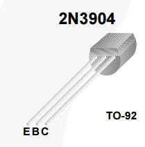
TO-92 Pinout:
Usually the same between models (also between NPN/PNP) but check your datasheet
Large Signal Model:
BJTs are current amplifying devices.
As seen in the large signal model below (NPN style - for PNP just flip everything), two electrodes (Base-Emitter) effectively act as a diode, while the other electrode (Collector) sinks current proportional to the Base-Emitter multiplied by a device-specific parameter Beta ($\beta$) (generally has a value ~200), also referred to as $h_{FE}$ the forward current transfer ratio.
$\beta$ is specified on the datasheet and is lower in PNP devices than NPN.
The emitter current is the sum of the base-emitter diode current
This predictable behavior makes BJTs convenient to use, understand, and analyze.
When analyzing a circuit with a BJT in forward-active mode, the two rules of thumb to remember are:
1) The device will try to maintain $V_{BE}$ at the PN junction diode forward potential (~0.7V)
2) The device will try to maintain $i_C=\beta *i_B$
In many cases the base current contribution to the emitter current can be ignored as a simplifying assumption (high $\beta$ means $I_E \approx I_C \gg I_B$ overwhelms the base contribution)

A BJT transistor with forward-biased $V_{BE}$ can only drive $V_{CE}$ so low, a condition referred to as saturation (not to be confused with the MOSFET saturation condition).
From a switching speed perspective, driving a BJT into saturation (low $V_{CE}$) can make "releasing" the switch (interrupting conduction) take a significantly longer amount of time - this is referred to as BJT "storage time" as charge carriers that build up in the base in saturation must be removed to allow the depletion region to form and cut off conduction.
This effect can be prevented by avoiding driving the transistor into saturation.
A clever circuit to "automatically" prevent this effect is the "baker clamp."
A simple implementation is to use a Shottky diode with low forward voltage drop with anode on the base and cathode on the collector - this holds $V_C$ within ~0.3V of $V_{B}$, which means $V_{CE}>0.4V$ which is sufficiently higher than typical saturation voltages $V_{CE(sat)} \approx 0.2V$.
No comments:
Post a Comment